


How much memory bandwidth should an AI accelerator have?
With each new generation of XPUs, the answer grows. High-bandwidth memory (HBM) now takes roughly 30% of the area of a typical accelerator die and, at 2026 memory prices, more than half of XPU cost.1 Every HBM generation adds bandwidth, and with it a wider interface, more power and more heat in the same package.
At the 2026 OCP Global Summit in San Jose, Marvell presented its view on why custom HBM benefits from being designed as a system. Moving logic into a custom base die can free silicon for compute, it also bring new challenging on a new heat source under the DRAM stack. Area, power and heat are linked, so they cannot be solved one at a time. Marvell focuses on co-designing the base die, the die-to-die (D2D) interface and the package thermals together, solving them as one system problem for custom HBM.
The Memory Interface Is Crowding the Compute Die
Per-stack HBM bandwidth has grown about 1.7x every two years. It went from 0.5 TB/s for HBM2E in 2020 to as much as 4.1 TB/s expected for HBM4E, an increase of roughly 8x.2 The industry got there two ways: more data I/Os and faster I/O speeds. HBM4 doubled the interface to 2,048 bits.3
That width has a cost. AI keeps pushing compute performance and memory bandwidth demand higher, while the HBM PHY and controller on the XPU consume die area, power and “beachfront,” the die edge where memory connects. More HBM stacks compete with compute logic for the same edge, and memory bandwidth is becoming a dominant factor in how far AI accelerators can scale.
HBM4 also moves the base die to a logic process, which opens the door to custom base dies. The industry is starting to adopt them, moving logic off the XPU to help accelerate both compute and memory bandwidth.
What Custom HBM Changes
The Marvell® custom HBM compute architecture places a custom base die under each DRAM stack and moves the memory controller off the XPU. A power and area optimized D2D PHY replaces the wide HBM PHY on the XPU shoreline.4 Depending on the XPU design, the freed silicon is designed to provide up to 25% more area for compute, room for up to 33% more HBM stacks, and up to 70% lower memory interface power, compared with an XPU using standard HBM.5 The narrower D2D PHY needs less beachfront, which is where the room for additional HBM stacks comes from.
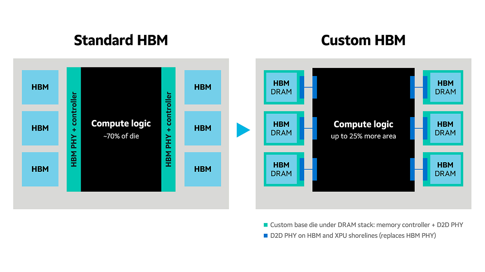
Figure 1: (Left) An XPU with standard HBM, where the HBM PHY and controller sit on the compute die. (Right) With custom HBM, the memory controller moves into a custom base die under each DRAM stack and a narrow D2D PHY connects the two, which can free up to 25% of the die for compute, depending on the XPU design. Top view, not to scale.
Logic Under the DRAM Makes Heat a First-order Constraint
Adding logic to the base die concentrates heat in a stack that was already hard to cool. In 2.5D packages, the HBM stack’s internal resistance accounts for 57% of its total thermal resistance, compared with 13% for the ASIC beside it.6 As stacks grow from 8-high to 16-high, internal temperatures are projected to exceed the thermal budget by 2028.6 That makes cooling the HBM stack itself as important as cooling the compute die.
Heat flux is rising at the same time. Next-generation HBM running above 28 Gbps is expected to exceed 2.0 W/mm². The hottest spot is the D2D PHY in the base die, which is also where custom HBM places its new logic.
No single component can address this alone. TIM, lid and cooling are best planned with the compute die, base die and package from the start. The biggest benefit of advanced cooling is resolving the hotspot near the D2D PHY.
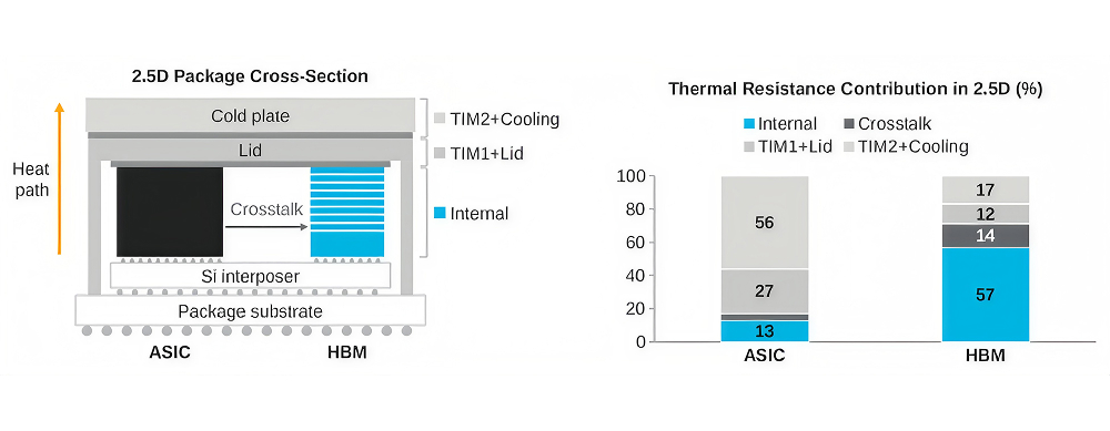
Figure 2: In a 2.5D package, internal resistance accounts for 57% of the HBM stack’s thermal resistance, compared with 13% for the ASIC. The stack, not the logic, is the limiter. Not to scale. Source: L. Park et al. (Samsung), “System-Level Thermal Validation of 2.5D Packages in GPU Servers,” IEEE ECTC 2026.
Three Ways the Industry Is Attacking Heat
Every pJ Saved in the D2D Interface Goes Back to Compute
For custom HBM, energy per bit sets the budget more than bandwidth density does. The larger gain is power. Adaptive power management tracks bursty data center traffic and can reduce interface power by up to 75% under normal workloads, and by up to 42% even at peak traffic, compared with an interface without adaptive power management.12 Savings are largest under bursty AI inference traffic. Power saved in the interface can become power available for compute or thermal headroom. The Marvell D2D interface is also ready for the next generation: an HBM5-class stack delivering 7.2 TB/s across a 9 mm beachfront needs about 6.4 Tbps/mm, and the Marvell 64 Gbps/wire bi-directional D2D interface is designed to deliver more than 30 Tbps/mm.12 That is nearly 5x the required bandwidth density, and the Marvell D2D interface is more than sufficient for next-generation HBM.
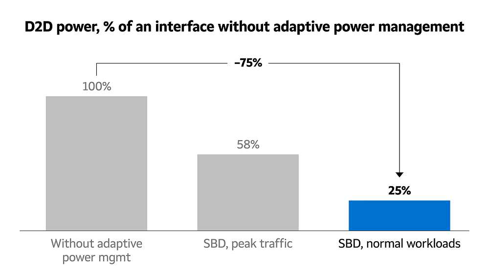
Figure 3: Adaptive power management in the Marvell 64 Gbps/wire D2D interface can reduce power by up to 75% under normal workloads and up to 42% at peak traffic, relative to an interface without it. Source: Marvell, Aug 2025.12
A Checklist for High-performance Custom HBM
Building It Together
No single company can build custom HBM alone. Memory makers, foundries, OSATs and XPU designers need to plan TIM, lid and cooling together. The open, collaborative model of the OCP community is a natural place to start, and Marvell looks forward to collaborating with companies across the chain to define and validate these building blocks.
References
###
This blog contains forward-looking statements within the meaning of the federal securities laws that involve risks and uncertainties. Forward-looking statements include, without limitation, any statement that may predict, forecast, indicate or imply future events or achievements. Forward-looking statements contained in this blog include, but are not limited to, statements regarding the expected benefits of custom HBM and the Marvell D2D interface, projected HBM bandwidth, heat flux and power trends, and future industry collaboration. Actual events or results may differ materially from those contemplated in this blog. Forward-looking statements are only predictions and are subject to risks, uncertainties and assumptions that are difficult to predict, including those relating to product development and performance, customer adoption and the timing of industry adoption of new technologies, and those described in the “Risk Factors” section of our Annual Reports on Form 10-K, Quarterly Reports on Form 10-Q and other documents filed by us from time to time with the SEC. Forward-looking statements speak only as of the date they are made. Readers are cautioned not to put undue reliance on forward-looking statements, and no person assumes any obligation to update or revise any such forward-looking statements, whether as a result of new information, future events or otherwise.
Marvell and the M logo are registered trademarks of Marvell and/or its affiliates. All other trademarks are the property of respective owners.
Tags: AI, , , AI infrastructure, ,