For massive AI workloads, purpose-built silicon consistently outperforms general-purpose architectures. Custom AI accelerators (XPUs) maximize performance-per-watt, expand usable memory per socket, and give hyperscalers unprecedented control over data center economics.
Marvell co-designs XPUs around specific workload and deployment requirements, combining customer-developed compute with Marvell IP across interconnect, memory, and packaging, supported by implementation expertise from architecture through production.
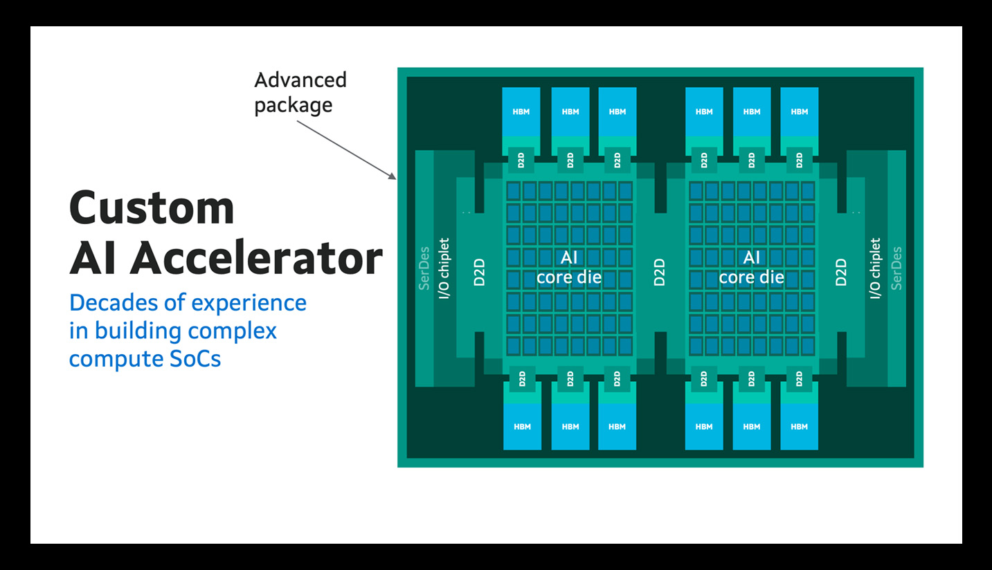
The accelerator is designed from a system perspective, balancing memory bandwidth, die partitioning, package architecture, scale-up connectivity, and rack-level requirements within a broader multi-vendor ecosystem.

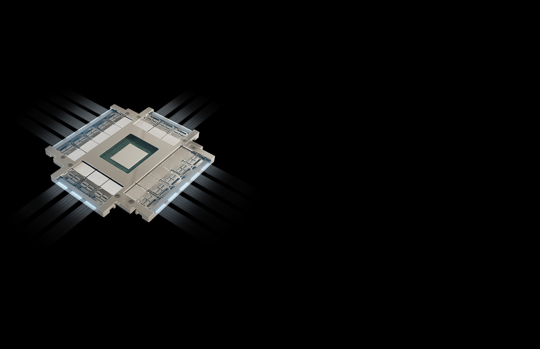
AI accelerators require high-speed interfaces to connect with scale-up fabrics, retimers, copper links, and optical systems. Marvell SerDes technology provides the electrical foundation for high-bandwidth accelerator connectivity.
This helps hyperscalers match accelerator I/O to the bandwidth, reach, and power requirements of the system.
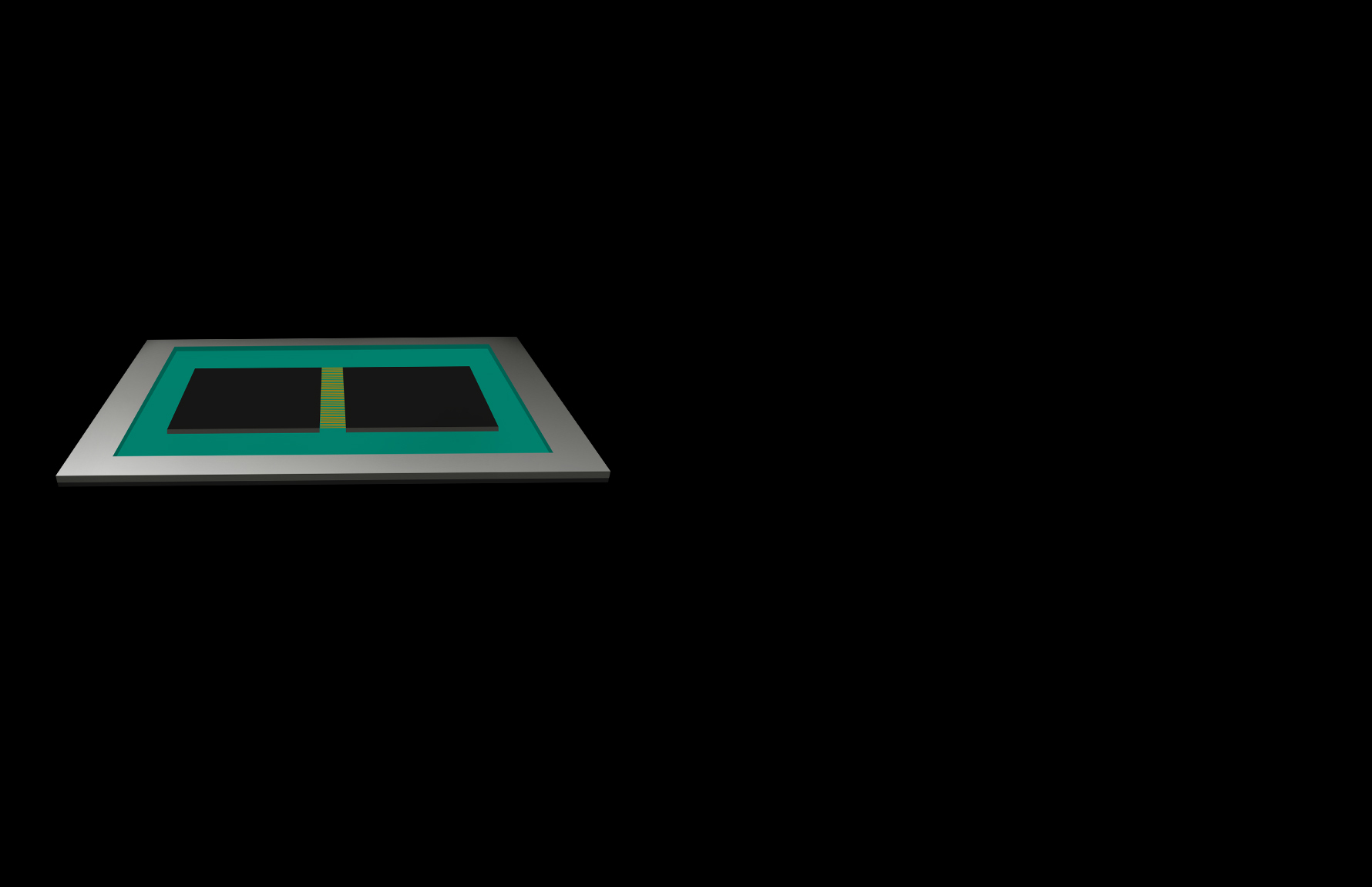
Scaling multi-die accelerators requires massive bandwidth between compute, memory, and I/O dies without exhausting power budgets or die-edge real estate. Marvell 2nm D2D IP delivers breakthrough efficiency.
By reducing the power and area required to move data between dies, Marvell die-to-die technology gives architects greater flexibility to partition accelerator functions across the package.
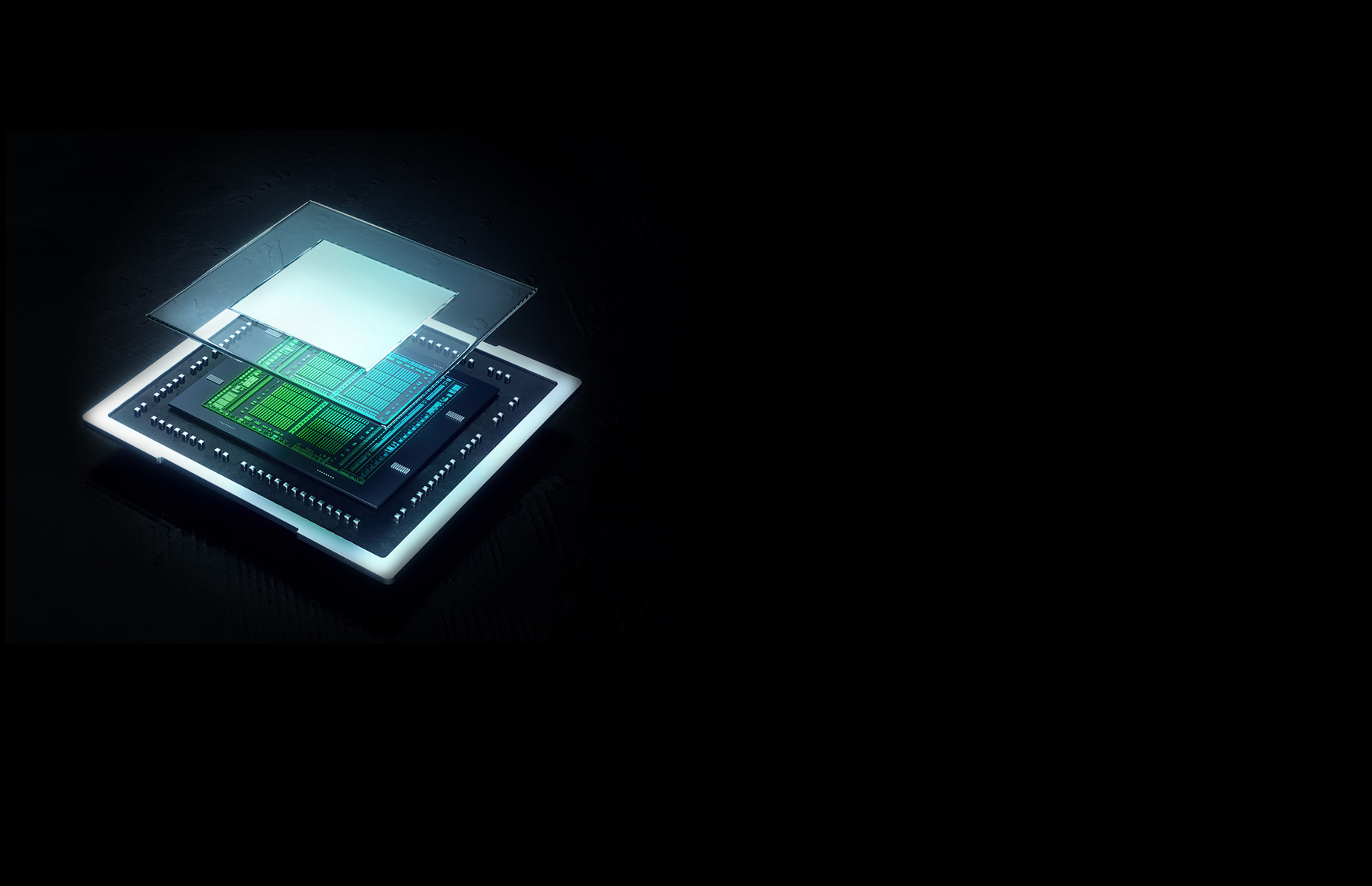
AI accelerators require substantial on-chip memory, but SRAM can consume significant die area and standby power. Marvell dense SRAM gives architects flexibility in how silicon and power are allocated across compute, memory, and workload-specific functions.
By reducing on-chip memory overhead, Marvell dense SRAM can free area and power for additional compute, larger memory capacity, or other accelerator-specific features.
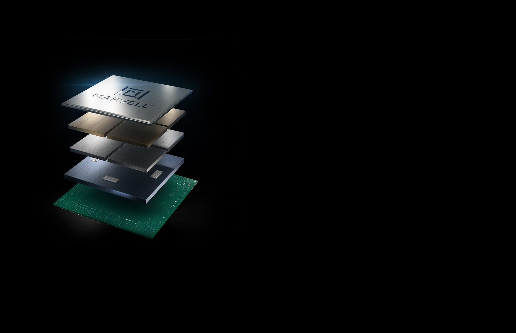
Reticle limits mean a single monolithic die can no longer hold enough compute, memory, and I/O for a frontier accelerator. Package architecture directly affects bandwidth, power delivery, thermals, yield, test, manufacturability, and supply. Marvell advanced packaging assembles multiple optimized dies into one accelerator that behaves as a single system.
Marvell makes packaging a first-order design choice, helping hyperscalers integrate more compute and memory while balancing performance, manufacturing, and supply.
Learn More
Learn More
Learn More

A workload-optimized compute engine that Marvell co-designs with a single hyperscaler, built as a multi-die system in a package. It integrates your IP with Marvell foundational IP, surrounded by high-bandwidth memory, dense on-chip SRAM, and high-speed I/O.
Hyperscalers operate AI workloads at volumes where architecture choices can materially affect performance, power, and economics. AI accelerators allow compute, precision, memory hierarchy, I/O, and packaging to be aligned with defined workload and deployment requirements.
Customer-developed compute can remain central to the accelerator. Marvell can provide selected chiplets, IP, packaging, implementation, and production expertise around that differentiated compute architecture.
Marvell can support design-to-spec, co-development, or a combination of both. This allows different parts of the accelerator to use different engagement models based on technical ownership, integration complexity, and customer priorities.
Memory hierarchy, die partitioning, I/O, power, and packaging affect one another. Early engagement allows these decisions to be evaluated together before physical boundaries and interfaces are fixed.
Marvell has demonstrated working TSMC 2nm silicon and developed 2nm technologies such as dense SRAM and high-bandwidth D2D. Development also extends to TSMC A14 for future accelerator generations.
Marvell combines D2D, SerDes, dense SRAM, advanced packaging, physical implementation, power, thermal, test, and manufacturing expertise to help integrate compute, memory, and I/O across multiple dies.
Accelerator I/O is considered in the context of scale-up fabrics, network interfaces, switching, copper links, and optical connectivity. This helps align the accelerator with the system where it must operate.
The accelerator moves through silicon bring-up, characterization, manufacturing test, package qualification, reliability testing, yield improvement, and production qualification. Marvell also helps coordinate supply dependencies such as HBM, substrates, packaging, and test capacity.
Through depth in verification and test: simulation, design verification, hardware emulation, DFT, shift-left test development, reliability testing, and package qualification. System-level test confirms the device performs its intended function in your system, which is distinct from manufacturing test.
We believe better partnerships help to build better technologies. Let’s connect and see what we can design together!
We will be in touch with you soon!