
By Michael Kanellos, Head of Influencer Relations, Marvell
Computer architects have touted the performance and efficiency gains that can be achieved by replacing copper interconnects with optical technology in servers and processors for decades1.
With AI, it’s finally happening.
Marvell earlier this month announced that it will integrate co-packaged optics (CPO) technology into custom AI accelerators to improve the bandwidth, performance and efficiency of the chips powering AI training clusters and inference servers and opening the door to higher-performing scale-up servers.
The foundation of the offering is the Marvell 6.4Tbps 3D SiPho Engine announced in December 2023 and first demonstrated at OFC in March 2024. The 3D SiPho Engine effectively combines hundreds of components—drivers, transimpedance amplifiers, modulators, etc.—into a chiplet that itself becomes part of the XPU.
With CPO, XPUs will connect directly into an optical scale-up network, transmitting data further, faster, and with less energy per bit. LightCounting estimates that shipments of CPO-enabled ports in servers and other equipment will rise from a nominal number of shipments per year today to over 18 million by 20292.
Additionally, the bandwidth provided by CPO lets system architects think big. Instead of populating data centers with conventional servers containing four or eight XPUs, clouds can shift to systems sporting hundreds or even thousands of CPO-enhanced XPUs spread over multiple racks based around novel architectures—innovative meshes, torus networks—that can slash cost, latency and power. If supercomputers became clusters of standard servers in the 2000s, AI is shifting the pendulum back and turning servers into supercomputers again.
“It enables a huge diversity of parallelism schemes that were not possible with a smaller scale-up network domain,” wrote Dylan Patel of SemiAnalysis in a December article.
By Michael Kanellos, Head of Influencer Relations, Marvell
What happened in semis and accelerated infrastructure in 2024? Here is the recap:
1. Custom Controls the Future
Until relatively recently, computing performance was achieved by increasing transistor density à la Moore’s Law. In the future, it will be achieved through innovative design, and many of those innovative design ideas will come to market first—and mostly— through custom processors tailored to use cases, software environments and performance goals thanks to a convergence of unusual and unstoppable forces1 that quietly began years ago.
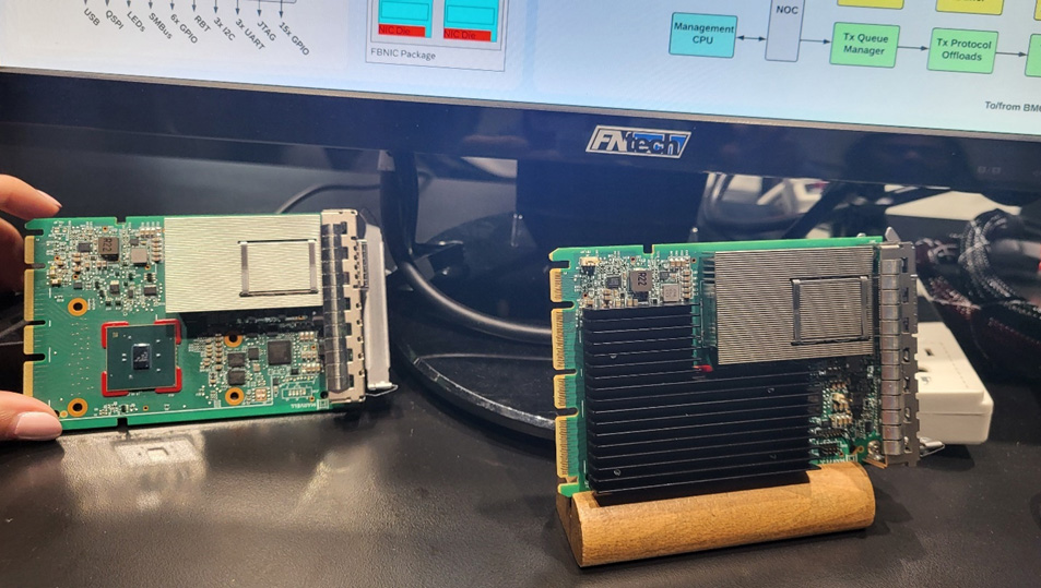
FB NIC on display at OFC
This article is part four in a series on talks delivered at Accelerated Infrastructure for the AI Era, a one-day symposium held by Marvell in April 2024.
Silicon photonics—the technology of manufacturing the hundreds of components required for optical communications with CMOS processes—has been employed to produce coherent optical modules for metro and long-distance communications for years. The increasing bandwidth demands brought on by AI are now opening the door for silicon photonics to come inside data centers to enhance their economics and capabilities.
What’s inside an optical module?
As the previous posts in this series noted, critical semiconductors like digital signal processors (DSPs), transimpedance amplifiers (TIAs) and drivers for producing optical modules have steadily improved in terms of performance and efficiency with each new generation of chips thanks to Moore’s Law and other factors.
The same is not true for optics. Modulators, multiplexers, lenses, waveguides and other devices for managing light impulses have historically been delivered as discrete components.
“Optics pretty much uses piece parts,” said Loi Nguyen, executive vice president and general manager of cloud optics at Marvell. “It is very hard to scale.”
Lasers have been particularly challenging with module developers forced to choose between a wide variety of technologies. Electro-absorption-modulated (EML) lasers are currently the only commercially viable option capable of meeting the 200G per second speed necessary to support AI models. Often used for longer links, EML is the laser of choice for 1.6T optical modules. Not only is fab capacity for EML lasers constrained, but they are also incredibly expensive. Together, these factors make it difficult to scale at the rate needed for AI.
By Radha Nagarajan, SVP and CTO, Optical and Copper Connectivity Business Group
The exponential increase in bandwidth demand will drive continuous innovation in, and deployment of, data movement interconnects for Cloud and Telecom providers. As a result, highly integrated silicon photonics platform solutions are expected to become a key enabling technology for the cloud and telecom market over the next decade.
What Does Highly Integrated Silicon Photonics Platform Mean for the Infrastructure Business?
As speed continues to go up, optical will replace copper as the primary conduit of the digital bits inside Cloud data centers. Marvell is investing heavily in silicon photonics to complement our high-speed CMOS technologies in data center interconnects to accelerate this transition.