
More customers, more devices, more technologies, and more performance—that, ultimately, is where custom silicon is headed. While Moore’s Law is still alive, customization is taking over fast as the engine for driving change, innovation and performance in data infrastructure. A growing universe of users and chip designers are embracing the trend and if you want to see what’s at the cutting edge of custom, the best chips to study are the compute devices for data centers, i.e. the XPUs, CPUs, and GPUs powering AI clusters and clouds. By 2028, custom computing devices are to account for $55 billion in revenue, or 25% of the market.1 Technologies developed for this segment will trickle down into others.
Here are three of the latest innovations from Marvell:
Multi-Die Packaging with RDL Interposers
Achieving performance and power gains by shrinking transistors is getting more difficult and expensive. “There has been a pretty pronounced slowing of Moore’s Law. For every technology generation we don’t get the doubling (of performance) that we used to get,” says Marvell’s Mark Kuemerle, Vice President of Technology, Custom Cloud Solutions. “Unfortunately, data centers don’t care. They need a way to increase performance every generation.”
Instead of shrinking transistors to get more of them into a finite space, chiplets effectively allow designers to stack cores on top of each other with the packaging serving as the vertical superstructure.
2.5D packaging, debuted by Marvell in May, increases the effective amount of compute silicon for a given space by 2.8 times.2 At the same time, the RDL interposer wires them in a more efficient manner. In conventional chiplets, a single interposer spans the floor space of the chips it connects as well as any area between them. If two computing cores are on opposite sides of a chiplet package, the interposer will cover the entire space.
Marvell® RDL interposers, by contrast, are form-fitted to individual computing die with six layers of interconnects managing the connections.
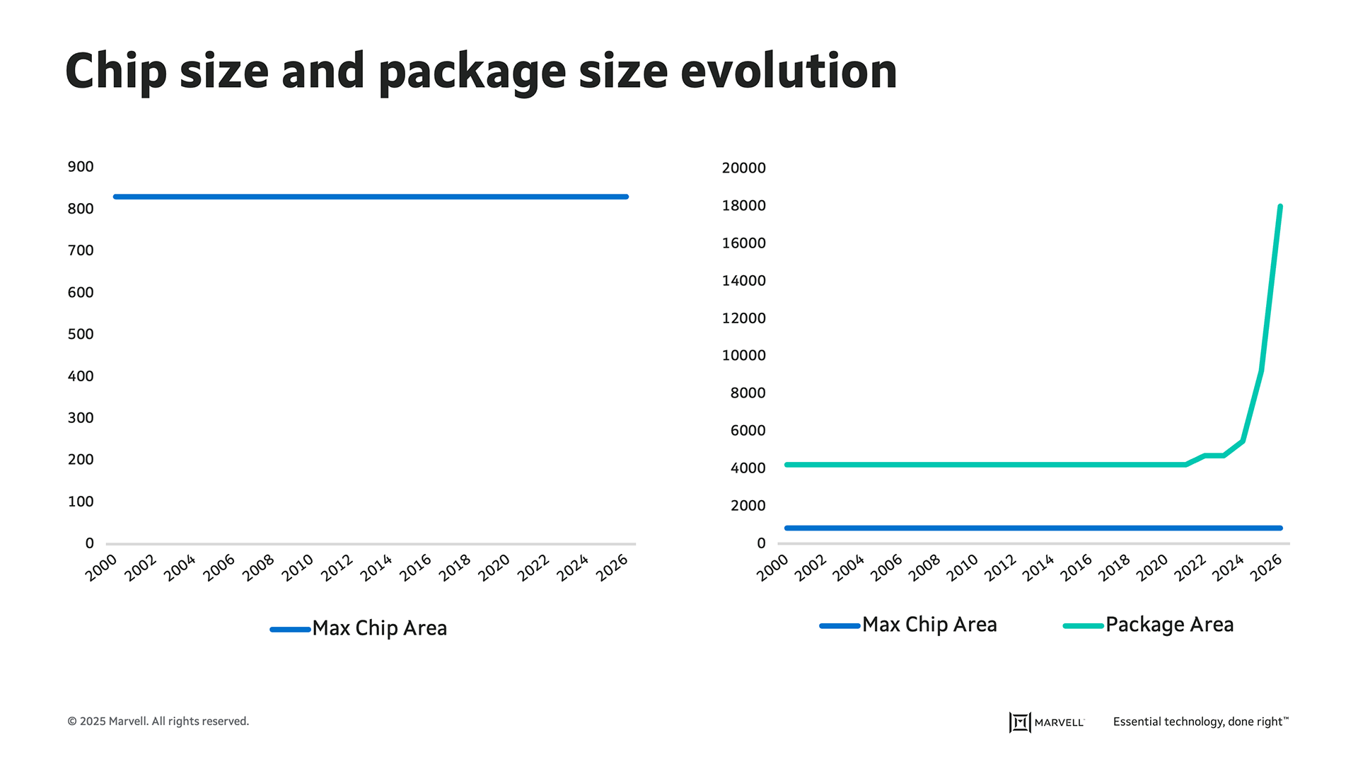
2.5D and multilayer packaging. With current manufacturing technologies, chips can achieve a maximum area of just over 800 sq. mm. By stacking them, the total number of transistors in an XY footprint can grow exponentially. Within these packages, RDL interposers are the elevator shafts, providing connectivity between and across layers in a space-efficient manner.
In all, the packaging provides headroom for 1390 mm2 of silicon and four stacks of high-bandwidth memory 3/3E (HBM3/3E). The Marvell multi-die packaging platform enables the integration of passive devices to reduce potential signal noise within the chiplet package caused by the power supply.
“A few years ago, advanced packaging used to be an afterthought. It has emerged as a key differentiator. It is as important as silicon, if not more,” said Mayank Mayukh, senior engineer of advanced packaging at Marvell. “This is a good time to be a packaging engineer.”
Custom SRAM (Static Random Access Memory)
“Memory” and “custom” are two words not often found together in computing. The large volumes, open nature of the commercial ecosystem, rapid transition to greater densities and incredible complexity of memory and storage have all guided the industry toward adhering to standards. AI is changing that.
With the highest bandwidth per square millimeter in the industry, Marvell custom SRAM enables chip designers to recover up to 15% of the total area of a 2nm design.3 Reducing the size of SRAM—the memory of choice for on-die caches—gives designers the freedom to add computing cores, increase memory, reduce the size or cost of a device, or a blend of all of the above to meet specific performance, power, use case or TCO goals. While most closely associated with CPUs, SRAM is also used in switches and other chips.
Marvell custom SRAM also consumes up to 66% less standby power compared to standard on-chip SRAM at equivalent densities while operating at speeds at up to 3.75 GHz.3
Custom SRAM is the third Marvell innovation for improving memory; each one targets different tiers of the memory hierarchy (see image below). In December 2024, Marvell unveiled custom HBM technology for reducing the space and power needed for the dense stacks of high-bandwidth memory (HBM) while increasing memory capacity by up to 33%.4 In July 2024, Marvell introduced the Structera family of CXL controllers[JB1] for adding terabytes of memory and supplemental computing capacity to cloud-based servers.5
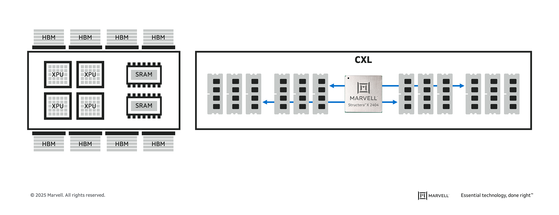
In the memory hierarchy, SRAM is typically integrated into the XPU die. While providing the smallest capacity, it’s the fastest memory repository and sits the closest to the XPU itself. HBM is in the XPU package and provides GBs of storage. The CXL sits on adjacent board and can provide TBs of storage, but it’s the furthest away from the XPU.
Package Integrated Voltage Regulation (PIVR)
Semiconductors are essentially miniature power grids. Electricity needs to be distributed across a heterogeneous landscape to different classes of “customers” (logic, I/O, etc.) at a range of voltages in real-time through a chaotic environment (heat and noise) across complex pathways. And, while power demand fluctuates unpredictably, power delivery needs to remain constant.
PIVR packaging essentially allows system designers to shift from using board-level power delivery systems—discrete subsystems made from several components typically situated several inches away from the processor on a printed circuit board—to smaller, faster, integrated silicon chips and passives tightly coupled with the processor.
The shift from on-board to in-package delivers a host of benefits. Shortening the power delivery path can reduce transmission losses by up to 85%, which increases the total power delivered by 15%.6 Integration also reduces board space, lowering system costs.
Close proximity also means greater power density—3 to 4 amperes per sq. mm versus 1.5 to 2 amperes per sq. mm for conventional solutions—for greater compute densities.6 Additionally, noise generated by power plummets (see the image below). Lower noise and greater density in turn paves the way for greater revenue per square foot per facility, and a better ROI. Put another way, IVR makes it possible to raise leading-edge chip power for leading-edge chips today from 500 to 1,200-watt levels to 4 kilowatt levels and use that power in a more efficient manner.6
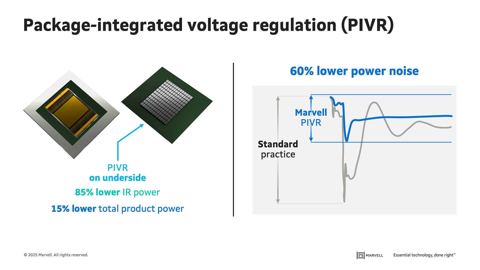
Typically, voltage regulators are situated far from the processor and on the underside of the board. With PIVR, they can be integrated into the underside of the chip package.
PIVR has appeared sporadically in the industry over the past decade, but improved technology combined with more urgent demands for better power distribution are bringing it to the forefront.
1. Marvell. Custom AI Investor Event, June 2025.
2. Marvell, May 2025.
3. Marvell, June 2025.
4. Marvell, December 2024.
5. Marvell, June 2024.
6. Marvell, June 2025.
# # #
This blog contains forward-looking statements within the meaning of the federal securities laws that involve risks and uncertainties. Forward-looking statements include, without limitation, any statement that may predict, forecast, indicate or imply future events or achievements. Actual events or results may differ materially from those contemplated in this blog. Forward-looking statements are only predictions and are subject to risks, uncertainties and assumptions that are difficult to predict, including those described in the “Risk Factors” section of our Annual Reports on Form 10-K, Quarterly Reports on Form 10-Q and other documents filed by us from time to time with the SEC. Forward-looking statements speak only as of the date they are made. Readers are cautioned not to put undue reliance on forward-looking statements, and no person assumes any obligation to update or revise any such forward-looking statements, whether as a result of new information, future events or otherwise.
Tags: data centers, AI, AI infrastructure, Optical Interconnect Packaging