
Plasmons have been used to accelerate drug discovery, enhance the sensitivity of sensors and even create artistic treasures in the Roman era.
Ongoing research at Marvell seeks to harness them to improve the performance of optical networks for the AI era. Plasmonics, a technology that leverages the properties of surface plasmon polaritons (SPPs), provides a promising pathway for enhancing the roadmap of silicon photonic (SiPho) light engines, a critical component inside optical modules.
Plasmonic-based SiPho light engines could support modules operating at 3.2T and beyond while consuming a fraction of the space and power per bit of modules based on existing technologies. Manufacturers could leverage foundry process technologies for scaling production.
SiPho, SPPs, and the Size of Light
SiPho light engines serve as bridges between the electrical and optical networks, helping ensure that data can pass between these two different realms rapidly and efficiently. Integrating hundreds of formerly discrete components into a single piece of silicon, SiPho devices dramatically reduced the cost, power and space of optical systems, contributing to the rise of pluggable optical networks. Module revenue is expected to reach $64 billion by 2031, more than triple total industry revenue in 2025.1
Modulators, one of the primary components of SiPho light engines, control the phase, amplitude and frequency of light encoded with data. Modulator size is governed by the diffraction limit, which dictates that light cannot be squeezed into a waveguide width of the order of half of its wavelength. Contemporary SiPho modulators typically measure 3,000 to 5,000 microns in length and operate at 60 GHz. Inside a module or chip package, this can constitute a sizeable amount of extremely valuable real estate.
SiPho modulators, while highly scalable and cost-efficient, are fundamentally constrained by the physical properties of light modulation in silicon, limiting their ability to scale efficiently to higher bandwidths. Without changes, future SiPho devices will struggle to provide the bandwidth needed for AI infrastructure.
Plasmonic waveguides address these challenges by compressing light below the diffraction limit at a metal-dielectric interface. These structures are integrated directly onto the silicon photonics platform, enabling the industry to build on the extensive foundation already established with SiPho while incorporating the performance advantages of plasmonics.
Plasmonic waveguides consist of a metal-dielectric channel filled with an active Pockels material integrated into SiPho devices or other photonic material system. At the metal-dielectric interface, free electrons in the metal couple strongly with incident laser light to form SPPs. The strong coupling effectively confines the light into dimensions far smaller than its own wavelengths and enhances the local electric field amplitude.
As a result, plasmonic devices can respond much faster to electrical signals, enabling much higher modulation rates than conventional photonic modulators. Plasmonic modulators also have a much higher modulation efficiency than conventional photonic modulators, making them naturally shorter. We have developed plasmonic modulator prototypes that measure approximately 10 microns in length, 300x to 500x shorter than existing SiPho devices and operate at 1THz, or more than 10x faster.2
This change in modulation exponentially increases bandwidth density: more data gets transmitted per second per square millimeter than with conventional photonic systems. While some signal loss occurs in the channel, the relatively short length of the modulator minimizes the impact on signal quality and bit error rates. At a high level, plasmonic devices combine micron-scale footprints and THz modulation speeds with the scale and economics of established silicon photonics, enabling designers to extend the capabilities of existing SiPho platforms without requiring a shift to new material systems. All these devices could be produced leveraging modified silicon processes with the metal dielectrics added toward the end of production.
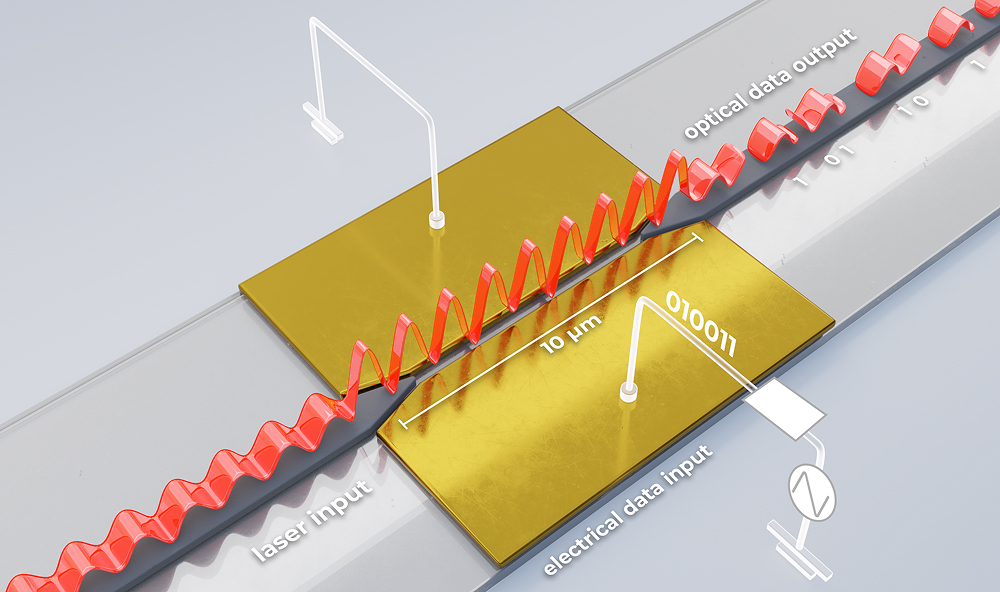
Top and side-view rendering of a plasmonic-based modulator. Source: Marvell, Polariton
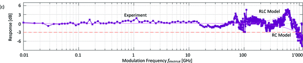
Experimental measurement of 1 THz EO electro-optic bandwidth of a plasmonic modulator.3
The increase in bandwidth density could be exploited in various ways. Plasmonic-based SiPho engines for co-packaged optics for scale-inside or scale-up applications could deliver the same or more bandwidth as conventional devices while minimizing space and power in these tightly constrained, latency-sensitive environments. The power, performance and space-saving characteristics of these devices make them an idea fit for the next generation of ultra compact, co-packaged optical interconnects.
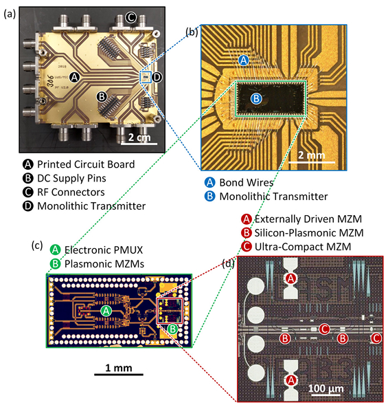
Diagram of the driver with the integrated plasmonic device with measurements for scale.4
At the other end of the application spectrum, plasmonic-based SiPho engines for scale-across networks could be used to develop compact, ultra-fast and energy efficient ZR/ZR+ class modules for scale-across networks that could carry more data further distances with less power. New classes of modules designed around massively parallel plasmonic arrays are another possibility. From a high level, these improvements could contribute to higher utilization, less network congestion and lower total cost of ownership across an infrastructure.
Life Sciences to Optics
Polariton, now part of Marvell, and ETH Zurich have researched the use of plasmonics for optical communications for over 15 years.5 In 2022, Polariton and ETH demonstrated that plasmonic-based modulators could operate at cryogenic temperatures needed for quantum computing, an area where conventional optics struggle.6 Last year, the companies set a world record with a demonstration of a 1.1 THz plasmonic modulator.7 High-speed SiPho devices capable of operating at 400G/lane containing plasmonic transponders were delivered to customers in 2026. This work now continues under Marvell.
The technology is still in the early days of development for commercialization. In the next phase, the focus is on improving the reliability and performance of the devices as well as manufacturing methodologies to make the devices at scale. Nonetheless, the results to date are quite promising. Expect to hear more about plasmonic technologies from Marvell in the future.
# # #
This blog contains forward-looking statements within the meaning of the federal securities laws that involve risks and uncertainties. Forward-looking statements include, without limitation, any statement that may predict, forecast, indicate or imply future events or achievements. Actual events or results may differ materially from those contemplated in this blog. Forward-looking statements are only predictions and are subject to risks, uncertainties and assumptions that are difficult to predict, including those described in the “Risk Factors” section of our Annual Reports on Form 10-K, Quarterly Reports on Form 10-Q and other documents filed by us from time to time with the SEC. Forward-looking statements speak only as of the date they are made. Readers are cautioned not to put undue reliance on forward-looking statements, and no person assumes any obligation to update or revise any such forward-looking statements, whether as a result of new information, future events or otherwise.
Tags: AI, Data Center, Optical Module, Coherent DSP, Networking