- 製品
- 会社概要
- サポート
- 製品
- タイプ別
- 市場別
コンピューティング
ネットワーキング
ストレージ
カスタム
- 会社概要
タイプ別
コンピューティング
ネットワーキング
ストレージ
市場別

Posts Tagged '112G SerDes'
-
March 02, 2023


Introducing the 51.2T Teralynx 10, the Industry’s Lowest Latency Programmable Switch
By Amit Sanyal, Senior Director, Product Marketing, Marvell
If you’re one of the 100+ million monthly users of ChatGPT—or have dabbled with Google’s Bard or Microsoft’s Bing AI—you’re proof that AI has entered the mainstream consumer market.
And what’s entered the consumer mass-market will inevitably make its way to the enterprise, an even larger market for AI. There are hundreds of generative AI startups racing to make it so. And those responsible for making these AI tools accessible—cloud data center operators—are investing heavily to keep up with current and anticipated demand.
Of course, it’s not just the latest AI language models driving the coming infrastructure upgrade cycle. Operators will pay equal attention to improving general purpose cloud infrastructure too, as well as take steps to further automate and simplify operations.
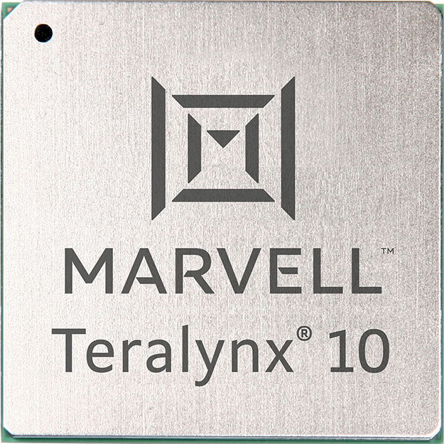
To help operators meet their scaling and efficiency objectives, today Marvell introduces Teralynx® 10, a 51.2 Tbps programmable 5nm monolithic switch chip designed to address the operator bandwidth explosion while meeting stringent power- and cost-per-bit requirements. It’s intended for leaf and spine applications in next-generation data center networks, as well as AI/ML and high-performance computing (HPC) fabrics.
A single Teralynx 10 replaces twelve of the 12.8 Tbps generation, the last to see widespread deployment. The resulting savings are impressive: 80% power reduction for equivalent capacity.
-
January 14, 2021
What’s Next in System Integration and Packaging? New Approaches to Networking and Cloud Data Center Chip Design
By Wolfgang Sauter, Customer Solutions Architect - Packaging, Marvel
The continued evolution of 5G wireless infrastructure and high-performance networking is driving the semiconductor industry to unprecedented technological innovations, signaling the end of traditional scaling on Single-Chip Module (SCM) packaging. With the move to 5nm process technology and beyond, 50T Switches, 112G SerDes and other silicon design thresholds, it seems that we may have finally met the end of the road for Moore’s Law.1 The remarkable and stringent requirements coming down the pipe for next-generation wireless, compute and networking products have all created the need for more innovative approaches. So what comes next to keep up with these challenges? Novel partitioning concepts and integration at the package level are becoming game-changing strategies to address the many challenges facing these application spaces.
During the past two years, leaders in the industry have started to embrace these new approaches to modular design, partitioning and package integration. In this paper, we will look at what is driving the main application spaces and how packaging plays into next-generation system architectures, especially as it relates to networking and cloud data center chip design.

最新の記事
- Infosec Global and Marvell partner to provide Crypto Agility in the Cloud
- HashiCorp and Marvell: Teaming Up for Multi-Cloud Security Management
- Cryptomathic and Marvell: Enhancing Crypto Agility for the Cloud
- The Big, Hidden Problem with Encryption and How to Solve It
- Self-Destructing Encryption Keys and Static and Dynamic Entropy in One Chip
アーカイブス
カテゴリ
- 5G (12)
- AI (11)
- 車載機器 (26)
- クラウド (7)
- コヒーレントDSP (2)
- 企業ニュース(100)
- カスタムシリコンソリューション (1)
- データセンター (39)
- データ処理ユニット (22)
- エンタープライズ (25)
- ESG (6)
- イーサネット・アダプター、コントローラー (12)
- イーサネット PHY (4)
- イーサネットスイッチ (30)
- ファイバーチャネル (10)
- Marvell Government Solutions (2)
- ネットワーク (31)
- Optical Modules (9)
- セキュリティ (3)
- Server Connectivity (15)
- SSD コントローラ (6)
- ストレージ (22)
- ストレージの推進者 (2)
- What Makes Marvell (22)

会社情報
リクルーティング情報
表示言語 (Language)
Copyright © 2024 Marvell, All Rights Reserved
- 利用規約
- プライバシーポリシー
- お問い合わせ先