
The exponential increase in bandwidth demand will drive continuous innovation in, and deployment of, data movement interconnects for Cloud and Telecom providers. As a result, highly integrated silicon photonics platform solutions are expected to become a key enabling technology for the cloud and telecom market over the next decade.
What Does Highly Integrated Silicon Photonics Platform Mean for the Infrastructure Business?
As speed continues to go up, optical will replace copper as the primary conduit of the digital bits inside Cloud data centers. Marvell is investing heavily in silicon photonics to complement our high-speed CMOS technologies in data center interconnects to accelerate this transition.
Evolution of Optical Interconnect Packaging
Fig 1 shows the evolution of high-speed optical interfaces in the last 20 years. Over this period, pluggable modules have dominated the optical interconnect space. The historical trend is impressive.
These remarkable achievements were realized through continuous improvements in electronics, optical components and packaging.
Light engines are the next phase of development in the ever-shrinking optical interface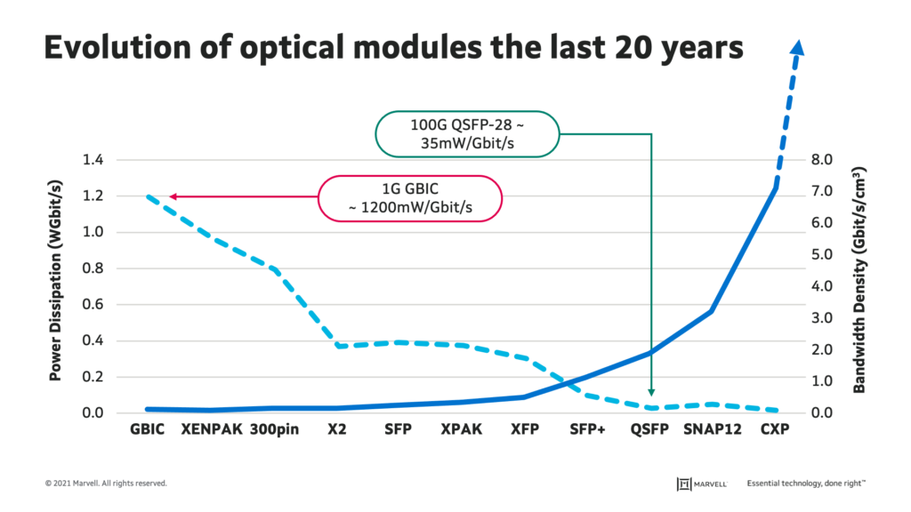 Fig. 1 Evolution of optical modules (adapted from Chap 14 in Optical Fiber Telecommunications Volume VIA, 2013.)
Integrated Light engine
In recent years there has been significant focus on heterogeneous integration on the silicon photonics platform.
With the switch capacity increasing from the current generation 12.8TBit/s to 51.2TBit/s in the near future, there is a need for low power, optical interconnects to be co-packaged near the switch to minimize power consumption. These miniaturized optical interconnects will be silicon photonics based and have the drive electronics and lasers heterogeneously integrated on the same substrate. This heterogenous integration will allow the performance of the electronics to be optimized independent of the photonics and will be critical for the highly integrated data center interconnect modules. Here we present details of such a light engine consisting of a silicon photonics substrate with the optical components, 2.5D heterogeneously integrated with InP DFB lasers, and modulator driver and transimpedance amplifier (TIA) made using SiGe technology.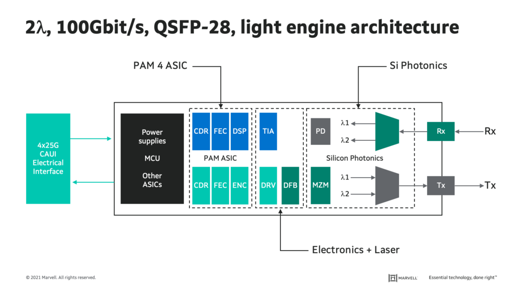 Fig. 2 shows the block diagram of the 2λ, 100Gbit/s, PAM4 light engine based on a highly integrated, silicon photonics optical chip and a PAM-4 DSP designed for intra- data center interconnects up to 80km reach. Here the TIA, driver and the DFB (shown in the red dashed box) are separate from the silicon photonics chip, and wire bonded to it. This is the basic architecture of the Marvell COLORZ® module. The light engine implementation of shrinking the footprint of a QSFP-28 module into a single integrated chip.
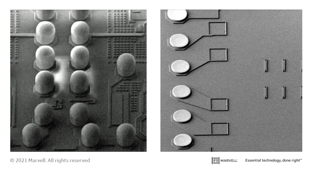 Fig. 3 The electronics were "bumped", and the silicon photonics was "plated"
To create the 2.5D integrated chip, the TIA and driver were first plated with Cu-Ni-SnAg bumps and then reflowed as shown on the left of Fig. 3, for the flip chip configuration. The pads on the silicon photonics chip, to which the electronics are attached, were CuNiAu plated as shown on the right of Fig. 3. AuSn solder was then deposited on the silicon photonics chip for the DFB laser attach. The TIA and driver were placed, using a high-accuracy flip chip bonder, on the re-designed silicon photonics chip and attached using a reflow oven at 260°C, using the standard SMT process.
The DFB lasers, at the CWDM wavelengths, were then attached to the light engine at a higher temperature for the AuSn solder. Single layer decoupling and bypass capacitors were also included on the silicon photonics substrate. This greatly simplifies the design of a light engine-based optical module.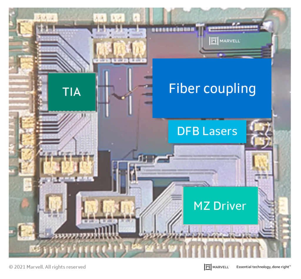 Fig. 4 2.5D light engine
This 2.5D assembly, in Fig 4, is more compact than what has been demonstrated to date, where the light engines comprise only of the light sources integrated on the silicon photonics substrate.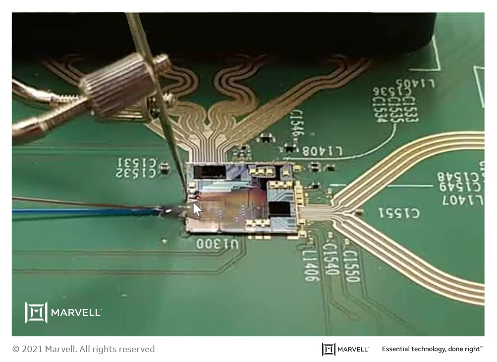 Fig. 5 Test setup for the light engine.
Fig 5 shows the setup to test the light engine. The PCB itself is simple; it only has RF traces and capacitors on them. A set of parallel fibers were epoxy attached to the light engine for the optical transmit output and receive input. The PAM-4 data is supplied via the RF cables (at the top of Fig 5). The TIA output is also connected out to the test equipment via a RF cable further to the right on Fig 4. The DFB lasers were biased using an external probe. They could have been wire bonded out like the TIA and driver.
The overall performance of the light engine was similar to the COLORZ module version, at a fraction of its size.
The race to deliver highly integrated, low power silicon photonic platforms for hyperscale data center interconnect applications is just getting started. The next generation will require continuous advancements in DSP, electronics, optics, and multi-dimensional integration.
Acknowledgments
I would like to thank the amazingly talented engineering team at Marvell and the various industrial partners for their contribution towards the realization of the light engine.
Open Compute Project Video Presentation
You can learn more about 2.5D heterogenous silicon photonics light engine during a presentation I gave at the 2020 OCP future technologies symposium, pre Inphi acquisition.
Tags: Hyperscale data centers, Optical Interconnect Packaging, Silicon Photonics, Silicon Photonics Light Engines, Silicon Photonics Platform