
By Michael Kanellos, Head of Influencer Relations, Marvell
The opportunity for custom silicon isn’t just getting larger – it’s becoming more diverse.
At the Custom AI Investor Event, Marvell executives outlined how the push to advance accelerated infrastructure is driving surging demand for custom silicon – reshaping the customer base, product categories and underlying technologies. (Here is a link to the recording and presentation slides.)
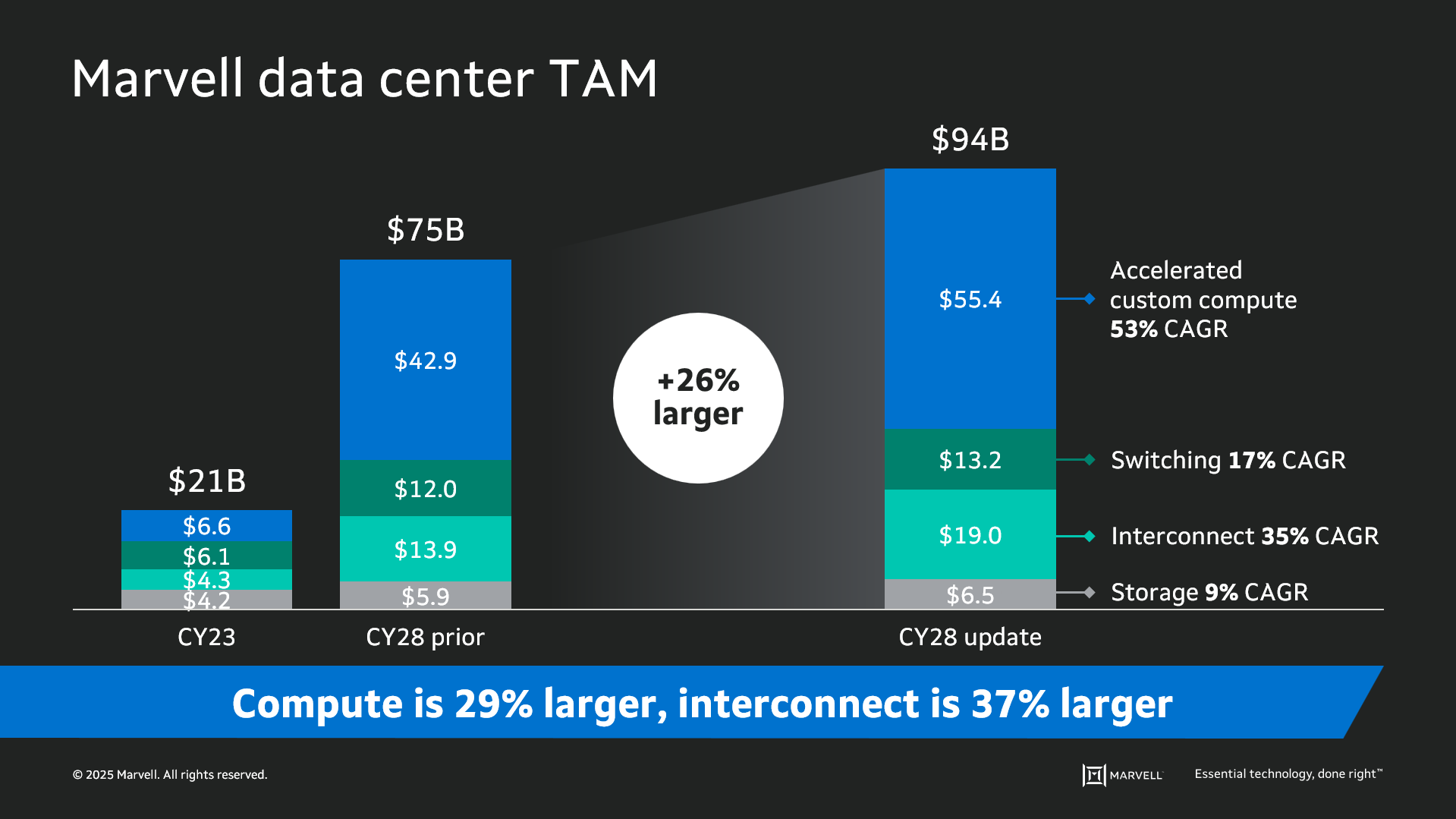
Data infrastructure spending is now slated to surpass $1 trillion by 20281 with the Marvell total addressable market (TAM) for data center semiconductors rising to $94 billion by then, 26% larger than the year before. Of that total, $55.4 billion revolves around custom devices for accelerated compute1. In fact, the forecast for every major product segment has risen in the past year, underscoring the growing momentum behind custom silicon.

The deeper you go into the numbers, the more compelling the story becomes. The custom market is evolving into two distinct elements: the XPU segment, focused on optimized CPUs and accelerators, and the XPU attach segment that includes PCIe retimers, co-processors, CPO components, CXL controllers and other devices that serve to increase the utilization and performance of the entire system. Meanwhile, the TAM for custom XPUs is expected to reach $40.8 billion by 2028, growing at a 47% CAGR1.
By Nicola Bramante, Senior Principal Engineer
Transimpedance amplifiers (TIAs) are one of the unsung heroes of the cloud and AI era.
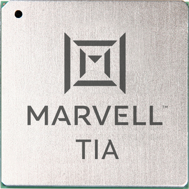
At the recent OFC 2025 event in San Francisco, exhibitors demonstrated the latest progress on 1.6T optical modules featuring Marvell 200G TIAs. Recognized by multiple hyperscalers for its superior performance, Marvell 200G TIAs are becoming a standard component in 200G/lane optical modules for 1.6T deployments.

TIAs capture incoming optical signals from light detectors and transform the underlying data to be transmitted between and used by servers and processors in data centers and scale-up and scale-out networks. Put another way, TIAs allow data to travel from photons to electrons. TIAs also amplify the signals for optical digital signal processors, which filter out noise and preserve signal integrity.
And they are pervasive. Virtually every data link inside a data center longer than three meters includes an optical module (and hence a TIA) at each end. TIAs are critical components of fully retimed optics (FRO), transmit retimed optics (TRO) and linear pluggable optics (LPO), enabling scale-up servers with hundreds of XPUs, active optical cables (AOC), and other emerging technologies, including co-packaged optics (CPO), where TIAs are integrated into optical engines that can sit on the same substrates where switch or XPU ASICs are mounted. TIAs are also essential for long-distance ZR/ZR+ interconnects, which have become the leading solution for connecting data centers and telecom infrastructure. Overall, TIAs are a must have component for any optical interconnect solution and the market for interconnects is expected to triple to $11.5 billion by 2030, according to LightCounting.
By Michael Kanellos, Head of Influencer Relations, Marvell
Computer architects have touted the performance and efficiency gains that can be achieved by replacing copper interconnects with optical technology in servers and processors for decades1.
With AI, it’s finally happening.
Marvell earlier this month announced that it will integrate co-packaged optics (CPO) technology into custom AI accelerators to improve the bandwidth, performance and efficiency of the chips powering AI training clusters and inference servers and opening the door to higher-performing scale-up servers.
The foundation of the offering is the Marvell 6.4Tbps 3D SiPho Engine announced in December 2023 and first demonstrated at OFC in March 2024. The 3D SiPho Engine effectively combines hundreds of components—drivers, transimpedance amplifiers, modulators, etc.—into a chiplet that itself becomes part of the XPU.
With CPO, XPUs will connect directly into an optical scale-up network, transmitting data further, faster, and with less energy per bit. LightCounting estimates that shipments of CPO-enabled ports in servers and other equipment will rise from a nominal number of shipments per year today to over 18 million by 20292.
Additionally, the bandwidth provided by CPO lets system architects think big. Instead of populating data centers with conventional servers containing four or eight XPUs, clouds can shift to systems sporting hundreds or even thousands of CPO-enhanced XPUs spread over multiple racks based around novel architectures—innovative meshes, torus networks—that can slash cost, latency and power. If supercomputers became clusters of standard servers in the 2000s, AI is shifting the pendulum back and turning servers into supercomputers again.
“It enables a huge diversity of parallelism schemes that were not possible with a smaller scale-up network domain,” wrote Dylan Patel of SemiAnalysis in a December article.
By Michael Kanellos, Head of Influencer Relations, Marvell
What happened in semis and accelerated infrastructure in 2024? Here is the recap:
1. Custom Controls the Future
Until relatively recently, computing performance was achieved by increasing transistor density à la Moore’s Law. In the future, it will be achieved through innovative design, and many of those innovative design ideas will come to market first—and mostly— through custom processors tailored to use cases, software environments and performance goals thanks to a convergence of unusual and unstoppable forces1 that quietly began years ago.

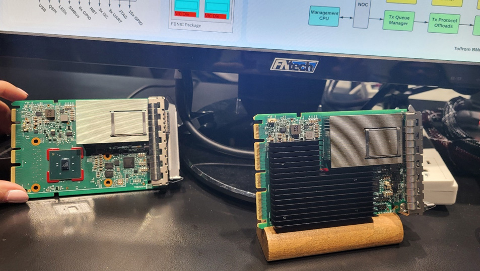
FB NIC on display at OFC
With AI computing and cloud data centers requiring unprecedented levels of performance and power, Marvell is leading the way with transformative optical interconnect solutions for accelerated infrastructure to meet the rising demand for network bandwidth.
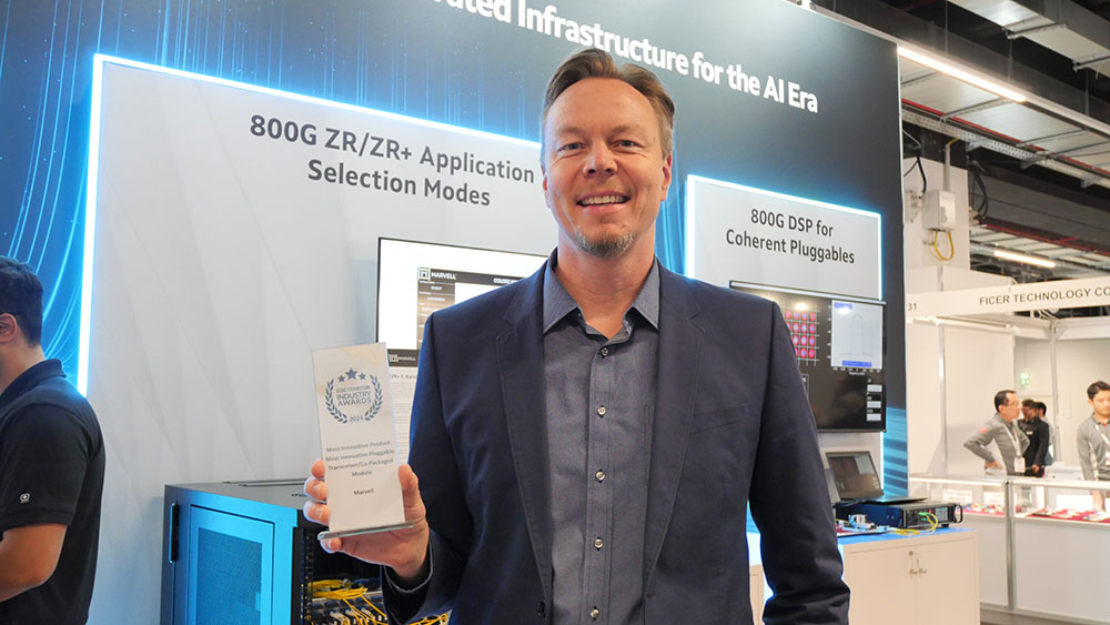
At the ECOC 2024 Exhibition Industry Awards event, Marvell received the Most Innovative Pluggable Transceiver/Co-Packaged Module Award for the Marvell® COLORZ® 800 family. Launched in 2020 for ECOC’s 25th anniversary, the ECOC Exhibition Industry Awards spotlight innovation in optical communications, transport, and photonic technologies. This recognition highlights the company’s innovations in ZR/ZR+ technology for accelerated infrastructure and demonstrates its critical role in driving cloud and AI workloads.
