Posts Tagged 'AI infrastructure'
-
June 18, 2024
Custom Compute in the AI Era
This article is the final installment in a series of talks delivered Accelerated Infrastructure for the AI Era, a one-day symposium held by Marvell in April 2024.
AI demands are pushing the limits of semiconductor technology, and hyperscale operators are at the forefront of adoption—they develop and deploy leading-edge technology that increases compute capacity. These large operators seek to optimize performance while simultaneously lowering total cost of ownership (TCO). With billions of dollars on the line, many have turned to custom silicon to meet their TCO and compute performance objectives.
But building a custom compute solution is no small matter. Doing so requires a large IP portfolio, significant R&D scale and decades of experience to create the mix of ingredients that make up custom AI silicon. Today, Marvell is partnering with hyperscale operators to deliver custom compute silicon that’s enabling their AI growth trajectories.Why are hyperscale operators turning to custom compute?
Hyperscale operators have always been focused on maximizing both performance and efficiency, but new demands from AI applications have amplified the pressure. According to Raghib Hussain, president of products and technologies at Marvell, “Every hyperscaler is focused on optimizing every aspect of their platform because the order of magnitude of impact is much, much higher than before. They are not only achieving the highest performance, but also saving billions of dollars.”
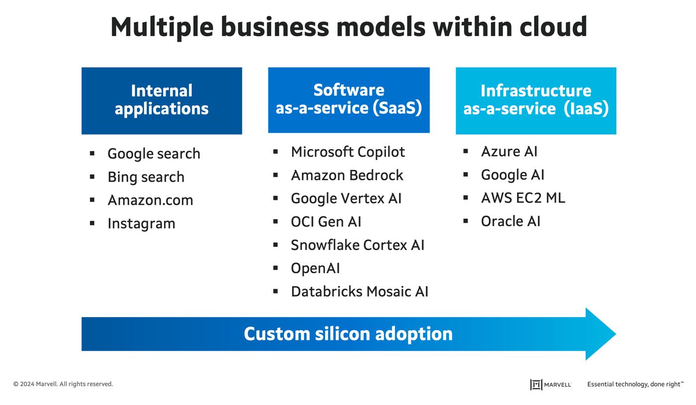
With multiple business models in the cloud, including internal apps, infrastructure-as-a-service (IaaS), and software-as-a-service (SaaS)—the latter of which is the fastest-growing market thanks to generative AI—hyperscale operators are constantly seeking ways to improve their total cost of ownership. Custom compute allows them to do just that. Operators are first adopting custom compute platforms for their mass-scale internal applications, such as search and their own SaaS applications. Next up for greater custom adoption will be third-party SaaS and IaaS, where the operator offers their own custom compute as an alternative to merchant options.

Progression of custom silicon adoption in hyperscale data centers.
-
June 11, 2024
How AI Will Drive Cloud Switch Innovation
This article is part five in a series on talks delivered at Accelerated Infrastructure for the AI Era, a one-day symposium held by Marvell in April 2024.
AI has fundamentally changed the network switching landscape. AI requirements are driving foundational shifts in the industry roadmap, expanding the use cases for cloud switching semiconductors and creating opportunities to redefine the terrain.
Here’s how AI will drive cloud switching innovation.
A changing network requires a change in scale
In a modern cloud data center, the compute servers are connected to themselves and the internet through a network of high-bandwidth switches. The approach is like that of the internet itself, allowing operators to build a network of any size while mixing and matching products from various vendors to create a network architecture specific to their needs.
Such a high-bandwidth switching network is critical for AI applications, and a higher-performing network can lead to a more profitable deployment.
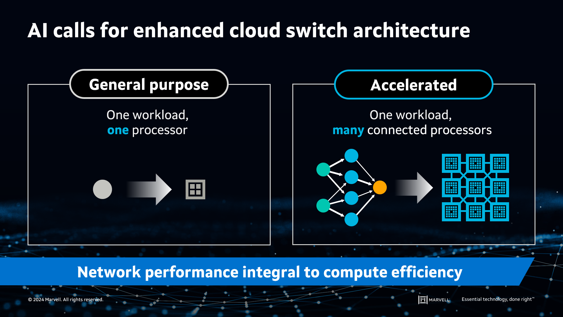
However, expanding and extending the general-purpose cloud network to AI isn’t quite as simple as just adding more building blocks. In the world of general-purpose computing, a single workload or more can fit on a single server CPU. In contrast, AI’s large datasets don’t fit on a single processor, whether it’s a CPU, GPU or other accelerated compute device (XPU), making it necessary to distribute the workload across multiple processors. These accelerated processors must function as a single computing element.

AI requires accelerated infrastructure to split workloads across many processors.
-
June 06, 2024
Silicon Photonics Comes of Age
This article is part four in a series on talks delivered at Accelerated Infrastructure for the AI Era, a one-day symposium held by Marvell in April 2024.
Silicon photonics—the technology of manufacturing the hundreds of components required for optical communications with CMOS processes—has been employed to produce coherent optical modules for metro and long-distance communications for years. The increasing bandwidth demands brought on by AI are now opening the door for silicon photonics to come inside data centers to enhance their economics and capabilities.
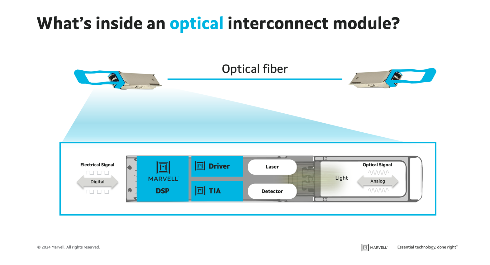
What’s inside an optical module?
As the previous posts in this series noted, critical semiconductors like digital signal processors (DSPs), transimpedance amplifiers (TIAs) and drivers for producing optical modules have steadily improved in terms of performance and efficiency with each new generation of chips thanks to Moore’s Law and other factors.
The same is not true for optics. Modulators, multiplexers, lenses, waveguides and other devices for managing light impulses have historically been delivered as discrete components.
“Optics pretty much uses piece parts,” said Loi Nguyen, executive vice president and general manager of cloud optics at Marvell. “It is very hard to scale.”
Lasers have been particularly challenging with module developers forced to choose between a wide variety of technologies. Electro-absorption-modulated (EML) lasers are currently the only commercially viable option capable of meeting the 200G per second speed necessary to support AI models. Often used for longer links, EML is the laser of choice for 1.6T optical modules. Not only is fab capacity for EML lasers constrained, but they are also incredibly expensive. Together, these factors make it difficult to scale at the rate needed for AI.
-
June 02, 2024
A Deep Dive into the Copper and Optical Interconnects Weaving AI Clusters Together
This article is part three in a series on talks delivered at Accelerated Infrastructure for the AI Era, a one-day symposium held by Marvell in April 2024.
Twenty-five years ago, network bandwidth ran at 100 Mbps, and it was aspirational to think about moving to 1 Gbps over optical. Today, links are running at 1 Tbps over optical, or 10,000 times faster than cutting edge speeds two decades ago.
Another interesting fact. “Every single large language model today runs on compute clusters that are enabled by Marvell’s connectivity silicon,” said Achyut Shah, senior vice president and general manager of Connectivity at Marvell.
To keep ahead of what customers need, Marvell continually seeks to boost capacity, speed, and performance of the digital signal processors (DSPs), transimpedance amplifiers or TIAs, drivers, firmware and other components inside interconnects. It’s an interdisciplinary endeavor involving expertise in high frequency analog, mixed signal, digital, firmware, software and other technologies. The following is a map to the different components and challenges shaping the future of interconnects and how that future will shape AI.
Inside the Data Center
From a high level, optical interconnects perform the task their name implies: they deliver data from one place to another while keeping errors from creeping in during transmission. Another important task, however, is enabling data center operators to scale quickly and reliably.
“When our customers deploy networks, they don’t start deploying hundreds or thousands at a time,” said Shah. “They have these massive data center clusters—tens of thousands, hundreds of thousands and millions of (computing) units—that all need to work and come up at the exact same time. These are at multiple locations, across different data centers. The DSP helps ensure that they don’t have to fine tune every link by hand.”

-
May 23, 2024
Scaling AI Means Scaling Interconnects
This article is part two in a series on talks delivered at Accelerated Infrastructure for the AI Era, a one-day symposium held by Marvell in April 2024.
Interconnects have played a key role in enabling technology since the dawn of computing. During World War II, Alan Turing used the Turing machine to perform mathematical computations to break the Nazi’s code. This fast—at least at the time—computer used a massive parallel system and numerous interconnects. Eighty years later, interconnects play a similar role for AI—providing a foundation for massively parallel problems. However, with the growth of AI comes unique networking challenges—and Marvell is poised to meet the needs of this ever-growing market.
What’s driving interconnect growth?
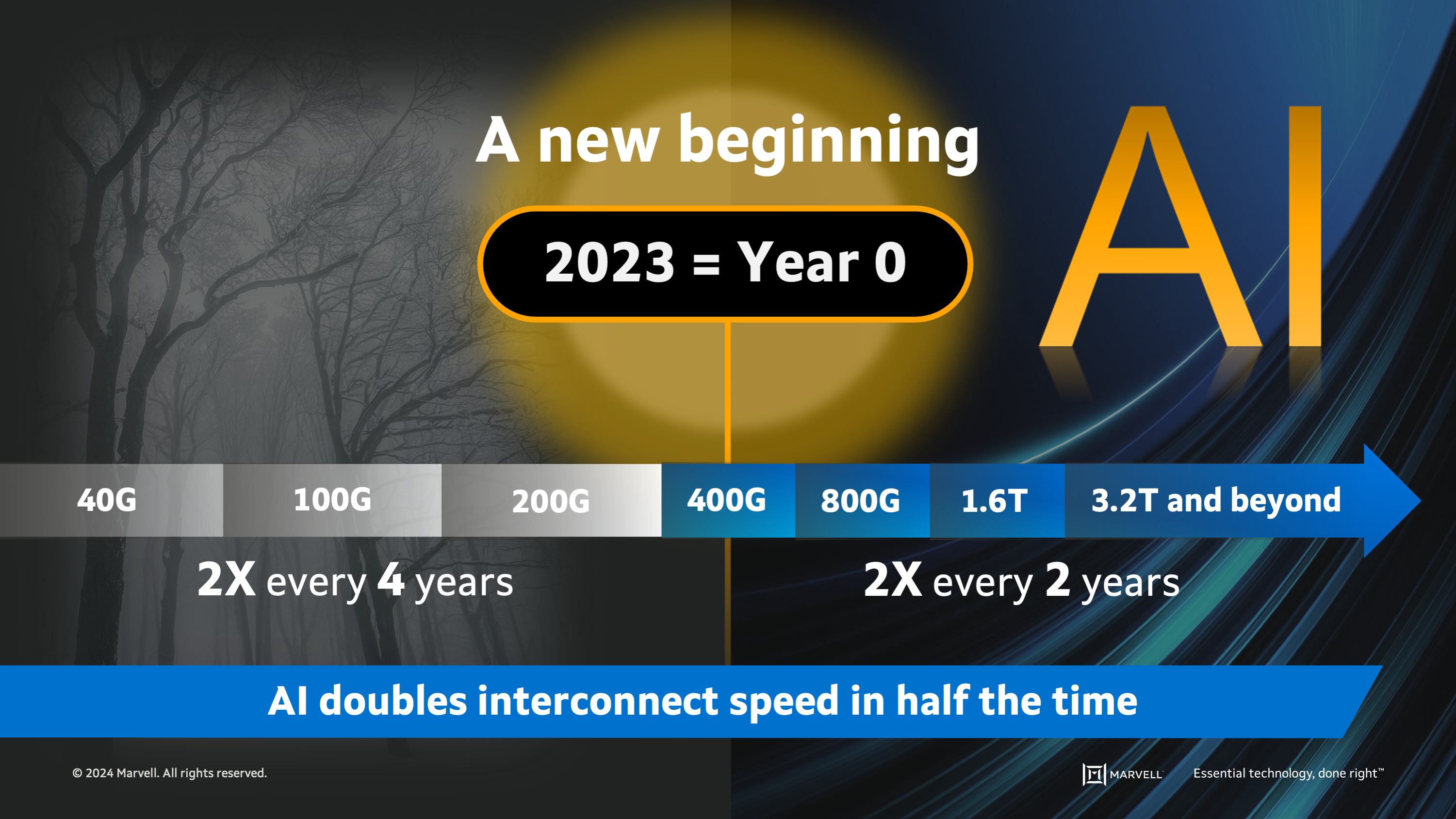
Before 2023, the interconnect world was a different place. Interconnect speeds were driven by the pace of cloud data center server upgrades: the upgrades occurred every four years so the speed of interconnects doubled every four years at the same time. In 2023, generative AI took the interconnect wheel, and demand for AI is driving speeds to double every two years. And, while copper remains a viable technology for chip-to-chip and other short reach connections, optical is the dominant medium for AI.“Optical is the only technology that can give you the bandwidth and reach needed to connect hundreds and thousands and tens of thousands of servers across the whole data center,” said Dr. Loi Nguyen, executive vice president and general manager of Cloud Optics at Marvell. “No other technology can do the job—except optical.”


